Skip to content

What Is a Solar Cell Carrier?

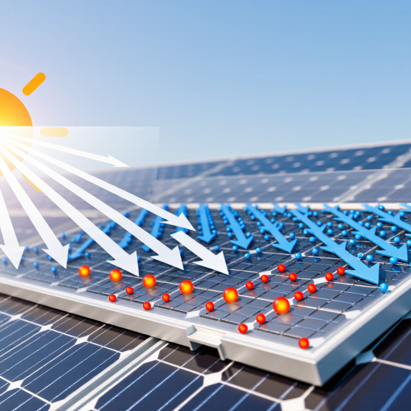
A solar cell does not turn sunlight into electricity in one step. Light absorbed by a semiconductor creates mobile charge carriers: electrons and positively charged “holes.” Their movement and collection at electrical contacts produce current. In practical terms, the carrier journey begins when a photon reaches the cell and ends at a contact—or through recombination, which wastes some of its energy.

This small-scale process matters across a rapidly expanding industry. The IEA PVPS Trends 2024 report estimates that global cumulative photovoltaic capacity reached about 1.6 terawatts by the end of 2023. The International Technology Roadmap for Photovoltaic (ITRPV), a recurring industry report, tracks manufacturing advances that influence how efficiently cells generate and collect carriers. These figures describe the market and technology landscape; they do not mean every cell performs equally. Materials, defects, temperature, and cell design all affect carrier lifetime and collection.

As photovoltaic researcher Dr. Martin A. Green’s work on solar-cell efficiency illustrates, better cell performance depends on limiting losses as well as absorbing light. A useful way to frame the challenge is: “A carrier must be generated, survive, and reach a contact.” That is a plain-language summary, not a direct quotation. It also leaves out a complication: real carriers do not follow neat, predictable paths. Understanding what a Solar Cell Carrier is—and how carriers move, recombine, and get collected—makes the cell’s operation easier to evaluate. The details are microscopic. The effect is measurable at the meter.
What Is a Solar Cell Carrier?

What Solar Cell Carriers Are: Electrons and Holes in Semiconductor Materials

In a solar cell, a carrier is a mobile charge that helps deliver electrical current. When silicon absorbs light, a photon can transfer energy to an electron. The electron moves into a higher-energy state, leaving behind a hole in the material’s electron structure. A hole is not a tiny physical particle. It behaves like a positive charge as nearby electrons move to fill the gap. That model is useful, though simplified.

Inside a silicon cell, electric fields near the junction help separate electrons and holes before they recombine. Electrons travel toward one contact; holes move toward the other. Their movement through an external circuit powers a load, such as a small fan. Recombination wastes some absorbed energy as heat or light. Tiny defects and impurities can change how often it happens. Real devices are messier than diagrams suggest.

Carrier collection helps explain why cell design matters, but it is only part of performance. The IEA PVPS report Trends in Photovoltaic Applications 2024 estimates global cumulative photovoltaic capacity reached about 1,624 gigawatts by the end of 2023. At that scale, small efficiency losses matter. NREL’s Best Research-Cell Efficiency Chart tracks certified results across cell technologies, offering a useful benchmark rather than a promise for everyday modules. A record cell and a rooftop panel are not the same thing. That gap deserves attention.

How Photons Create Electron–Hole Pairs Above Silicon’s 1.12 eV Band Gap

What Is a Solar Cell Carrier?

How Photons Create Electron–Hole Pairs Above Silicon’s 1.12 eV Band Gap

In silicon, a photon must carry roughly 1.12 electron volts to bridge the band gap at room temperature. That energy lifts an electron from a lower-energy state into one where it can move through the crystal. The missing electron leaves a positively charged hole behind. Together, they form an electron–hole pair, often called a carrier pair. A 1.12 eV photon has a wavelength near 1,107 nanometers; shorter-wavelength photons generally have more energy. Not every photon counts. Below the band gap, silicon usually cannot absorb a photon to create this pair.

Once created, electrons and holes move through the cell. An internal electric field helps separate them, while contacts collect charge to produce current. Excess photon energy usually becomes heat, not extra electrical output. Defects can also make carriers recombine before collection. Real silicon is messier. Fraunhofer ISE’s Photovoltaics Report (2024) estimates crystalline silicon made up about 97% of global solar-cell production in 2023, so this process matters at industrial scale. IEA PVPS’s Trends 2024 report estimates that around 447 GW of photovoltaic capacity was added worldwide in 2023. Those figures describe deployment, not how efficiently each photon becomes current—a distinction worth keeping clear.

How a p–n Junction’s Built-In Field Separates Charge Carriers

A solar-cell carrier is a mobile charge: an electron or a hole, the vacancy an electron leaves behind. Sunlight supplies energy to create electron–hole pairs in a semiconductor. At the p–n junction, electrons diffuse toward the p side and holes toward the n side, leaving charged atoms behind. This creates a built-in electric field across the depletion region. The field pushes electrons toward the n side and holes toward the p side.

That is the key. The field separates carriers; it does not supply their energy. Photons do that. Once separated, carriers can travel through the contacts and an external circuit. But carriers generated far from the junction must diffuse there first, and some recombine along the way. Not every carrier survives. A clean textbook diagram hides this messy detail.

The scale makes these losses matter. IEA PVPS reported more than 1.6 terawatts of installed global photovoltaic capacity by the end of 2023 in its Snapshot of Global PV Markets 2024. NREL’s Best Research-Cell Efficiency Chart records a 27.6% benchmark for crystalline-silicon research cells. These figures measure deployment and cell performance, not the junction field alone. Still, they show why efficient carrier separation matters. A stronger field is not automatically better; material quality, junction design, and recombination also shape the result. The simplified picture is useful, but incomplete.

How Silicon Carrier Mobility at 300 K Affects Charge Transport

What Is a Solar Cell Carrier?
How Silicon Carrier Mobility at 300 K Affects Charge Transport

A carrier is a mobile electron or hole that transports electrical charge through a solar cell. In crystalline silicon near 300 K, lightly doped material can have electron mobility around 1,350 cm²/V·s and hole mobility near 450 cm²/V·s. Electrons generally move faster. These figures describe idealized conditions, not every finished device.

Mobility links an applied electric field to drift speed: higher mobility usually means carriers cross a given region faster. In a working cell, light creates electron–hole pairs; the junction’s electric field separates them, while diffusion helps carriers reach the junction from regions with weaker fields. Faster transport can reduce the time carriers spend vulnerable to recombination. Timing matters.

But mobility is not a direct measure of cell efficiency. Doping, temperature, crystal defects, and strong electric fields can change it. High doping often lowers mobility through increased scattering. A carrier may also travel poorly if defects trap it. A clean textbook number is useful, but incomplete. Real cells show these trade-offs in measured current and voltage, not mobility alone.

At 300 K, low-field electron mobility in silicon is approximately 1,350 cm²/(V·s), while hole mobility is approximately 450 cm²/(V·s). Higher mobility generally means a carrier can drift faster under the same electric field. Actual values vary with factors such as doping and material conditions.

How Carrier Recombination Limits Output and the 33.7% Single-Junction Efficiency Limit

What Is a Solar Cell Carrier?

A solar cell carrier is an electron or a positively charged hole that moves through a semiconductor. Sunlight can lift an electron into a higher-energy state, leaving a hole behind. The pair may travel toward opposite contacts and contribute to electrical current. But they do not always make it. An electron can fall back into a hole before either reaches a contact; this process is called recombination. Defects, grain boundaries, and poorly controlled surfaces can make that loss more likely. Tiny details matter.

Recombination limits output because fewer carriers arrive at the contacts to deliver current. In silicon, for example, surface defects can act like meeting points where electrons and holes disappear from useful circulation. Good passivation reduces these losses, though it cannot eliminate every mechanism. Some recombination is unavoidable, even in an ideal cell. That point is easy to miss.

The commonly cited 33.7% single-junction limit comes from detailed-balance theory, not from one manufacturing flaw. It describes an ideal cell under standard sunlight assumptions, with an optimal bandgap near 1.34 electron volts. Photons below the bandgap pass through, while excess photon energy becomes heat; radiative recombination also sets a fundamental voltage loss. Real cells fall short because of additional optical, electrical, and material losses. The exact comparison depends on the conditions used, so the number is a benchmark, not a promise. A cleaner surface helps, but it cannot change the basic trade-offs.